Heavy Copper PCB Purchase Specification and Acceptance Evidence Guide
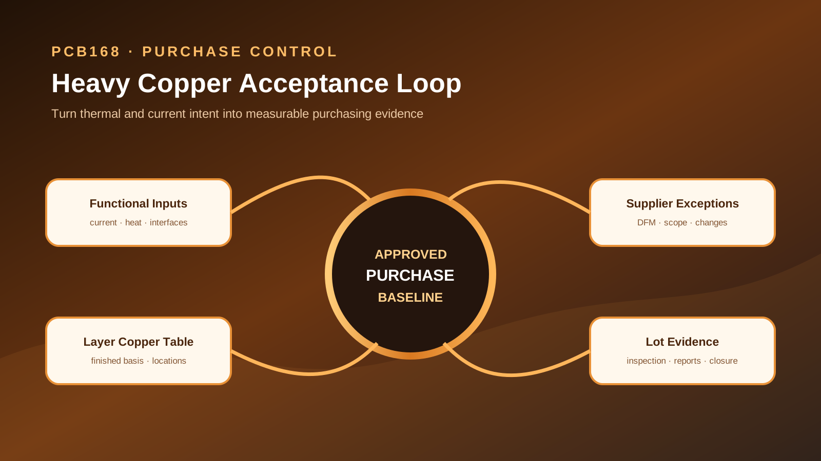
A heavy copper PCB purchase order that states only copper weight and overall board thickness does not preserve the design intent. The functional requirement may concern temperature rise on a power path, voltage drop at a connector, local heat spreading, a bolted interface or reliability under a defined operating environment. When purchasing reduces that context to one copper number, its relationship to routing geometry, holes, dielectric structure, surface finish and inspection method disappears. The supplier may quote one interpretation while incoming quality later applies another.
A useful purchase specification translates approved engineering intent into requirements that both parties can manufacture, measure and document. It does not replace electrical or thermal analysis, and it should not use a generic online current table as project validation. The workflow below connects design input, RFQ response, first-article review, routine acceptance and change control. Begin with the heavy copper PCB product page for project communication and use the PCB thermal management guide for general background. No PCB168-owned copper capability, equipment, certification, capacity, lead-time or customer-case claim is made here.
1. Record functional conditions before freezing copper
State what the heavy copper region is expected to do: carry continuous or transient current, spread heat, support a terminal or busbar interface, connect a power component, or serve another approved function. A current path may also require a waveform, allowable temperature-rise basis, ambient and cooling conditions, neighboring heat sources, routing layer, trace width and length, via array and connector interface. A thermal path may require heat-source location, boundary conditions, contact material and external heat-removal structure.
These inputs cannot be compressed into a universal “safe current” value. IPC-2152 and related engineering methods can support evaluation, but temperature depends on the complete construction and operating environment. The purchase specification should reference an engineering-approved copper and geometry definition rather than asking the fabricator to design the path from current alone. If the functional conditions are provisional, label the quotation as budgetary and repeat the review after design freeze.
2. Define copper by layer, location and measurement basis
“Copper thickness” may refer to starting foil, base copper, processed finished copper, plated copper, or a local cross-section. In a heavy copper structure, etching and plating results also vary by feature and location; one vague nominal cannot represent every point. List the requirement by layer and identify whether it applies to inner copper, outer copper, hole wall or a defined local feature. Reference the agreed measurement method, location, sampling plan and acceptance document.
Do not treat a foil supplier's nominal material value as automatic proof of finished copper at any position on the board. Do not mix weight and thickness expressions without identifying the conversion basis. If design requires a minimum finished copper result, state it in the fabrication drawing or controlled specification. If only starting copper is controlled, state how the finished board will be accepted. Any proposed construction change should appear in an exception list for design and quality review.
3. Review spacing, holes and dielectric filling as one structure
As copper becomes thicker, pattern formation, spacing, pad geometry and dielectric filling face a different set of constraints. The RFQ should expose controlled minimum trace width, spacing, copper-to-edge and copper-to-hole relationships, pad and hole geometry, and filling expectations between large copper features. A buyer should not infer project manufacturability from a generic product page or disclose dense local features only after quotation.
For each hole family, define finished-hole or drill terminology, the source of plating requirements, connected layers, current-carrying or thermal function, press-fit or mechanical use where applicable, and the surrounding copper and solder-mask conditions. If a parallel via array is part of an electrical or thermal path, design must control its count, location and connectivity. The fabricator may identify DFM risk but should not alter that path without approval. The multilayer PCB stackup guide provides useful context for organizing layer information.
4. Put thermal interfaces in the procurement drawing
Heavy copper does not automatically solve thermal performance. Board-level spreading also depends on dielectric, copper distribution, vias, component lands, enclosure, thermal interface materials and airflow. Mark heat-source regions, critical copper planes, contact surfaces, keep-open or keep-coated areas, mounting features and enclosure datums in the procurement package. If the mechanical drawing, PCB drawing and thermal model use different coordinates or revisions, reconcile them before RFQ release.
Where the board contacts a heat sink, baseplate or enclosure, identify the controlling source for flatness, finish, solder-mask opening, local height and cleanliness without inventing a universal tolerance. Each interface requirement needs a measurable location and approved criterion. The article on AI servers and heavy copper PCBs offers application context, but it must not be used as the numerical current, temperature-rise or acceptance basis for a specific product.
5. Freeze finish and assembly boundaries during quotation
The board may mate with terminals, press-fit hardware, soldered components or mechanical fasteners. State the surface finish, any selective finish, solder-mask coverage and openings, identification marks, connector-zone profile, and special cleanliness or packaging requirements for downstream assembly. If large copper areas, step changes or local geometry may affect mask coverage or assembly, expose those regions during DFM rather than after purchase.
Require the supplier's quotation to state material and stackup assumptions, copper terminology, panel basis, testing, report scope and exceptions. Purchasing should not compare totals without comparing scope. A quote that excludes an agreed microsection, dimensional report or controlled packaging requirement is not equivalent. When submitting through the quotation page, include a clause matrix and request a response to each requirement instead of relying on a narrative email.
6. Define first-article and routine-lot evidence
Separate design validation, first-article confirmation and routine lot inspection. A first article may confirm construction, critical cross-sections, dimensions, appearance, finish and functional interfaces. Routine inspection then follows the approved control plan. Before purchasing, decide which reports accompany each lot, which records the manufacturer retains, and what additional evidence is supplied when an exception occurs.
A microsection supplies evidence about a defined sampled location; it does not automatically represent every feature on every board. Visual inspection can identify observable anomalies but cannot replace a dimensional or structural measurement required by the specification. Electrical test demonstrates continuity and isolation under its defined method, not validated thermal performance. Each type of evidence answers a different question. The PCB quality inspection methods guide provides a broader hierarchy, while the order must define the actual sampling and acceptance basis.
7. Match documents, product and changes at incoming acceptance
Incoming review starts by matching the purchase order, PCB part number, revision, delivered quantity and package identity. Then confirm that each shipment document references the same lot and controlled specification. A report should identify the inspected item, characteristic, method or procedure, result, disposition and date. The existence of a report is not enough. If it covers a broad material family, another thickness or an obsolete drawing, the scope requires clarification.
Check whether material, stackup, foil, process route or inspection method changed during the order. Every approved deviation should have an identifier, applicable lot and expiry condition; it must not become an undocumented permanent relaxation. If a nonconformance appears, segregate the affected material, record facts and locations, preserve evidence, and let the responsible cross-functional team decide rework, concession, return or further analysis. Do not rewrite the receiving criterion to fit the delivered board.
8. Preserve a closed record for repeat orders
The complete record includes the approved specification, quotation exceptions, DFM questions and answers, purchase revision, manufacturer acknowledgement, first-article evidence, lot reports, nonconformance disposition and subsequent changes. A repeat order should start from the latest approved baseline, not from a copied old order patched by email. A change in current, cooling hardware, connector, layout or enclosure should trigger specification review even if the commercial part name remains similar.
The final release test can be reduced to four questions. Are the functional inputs clear? Does copper and construction have one measurement meaning? Does each acceptance record map to a requirement? Are deviations and changes closed? Only when all four are answered does purchasing receive a comparable and traceable heavy copper PCB rather than an unverified product label.
FAQ
Can a heavy copper PCB order specify only copper and board thickness? It should not. Define copper by layer and measurement basis, then connect it to current or thermal conditions, geometry, holes, finish, dimensions, inspection method and reporting.
Does a supplier material certificate prove finished copper thickness? Not automatically. A material document has its own scope. Finished copper must be verified at the locations, by the methods, sampling and criteria agreed in the order.
Does thicker copper always improve current capacity and cooling? No universal conclusion is valid without geometry, dielectric, interfaces, cooling and environment. Engineering must evaluate and validate the complete structure; purchasing orders the approved result.
Does an accepted microsection prove every location in the lot is acceptable? It proves the defined sampled section. Its representative scope is controlled by the agreed quality plan and contract, not expanded without evidence.
Can an approved deviation automatically carry into the next lot? No. State the part, revision, lot, quantity and expiry. A permanent change belongs in formal engineering change control and the purchasing baseline.
Sources
- IPC-2152, general methodology framework for evaluating current-carrying capacity in printed-board conductors; project temperature conclusions still require actual construction and environmental analysis.
- IPC-2221, generic printed-board design framework.
- IPC-6012, qualification and performance specification framework for rigid printed boards; class, revision and addenda are defined by the order.
- IPC-A-600, illustrated acceptability reference for printed boards; it does not replace project sampling and contractual criteria.
- Customer-approved electrical and thermal analysis, stackup, fabrication drawing, mechanical interface drawing, control plan and procurement specification.
Need PCBs for Your Project?
Get an instant quote — prototypes from $2, delivered worldwide.
Get Instant Quote