Heavy Copper PCB Manufacturers: 6 Process Evidence Requests Before You Award
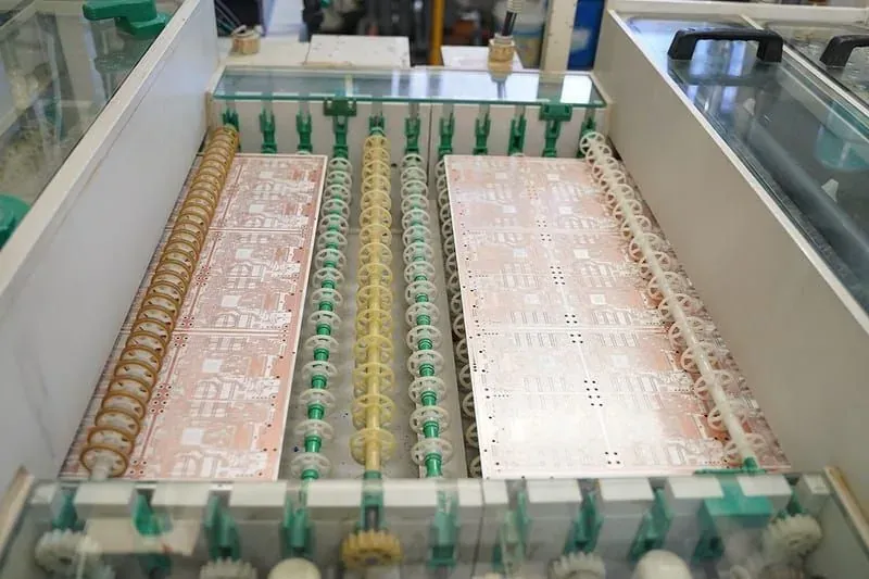
Why quote sheets cannot tell heavy copper capability apart
A quote is a commercial document assembled from a small number of fields. Copper weight enters it as a material cost and a yield assumption. Layer count enters it as lamination cycles. Board thickness enters it as material and drilling. What never enters it is the sequence of decisions that make a heavy copper build come out to specification.
That matters because heavy copper is not standard fabrication with more metal. Three things change at once:
- Etching stops being geometrically neutral. Thicker copper takes longer to etch through, so the sidewall slopes and the top of the conductor loses width. The artwork has to be compensated for that before tooling, and the compensation depends on the copper weight and the etch line.
- Lamination has to fill a much larger step. Between a heavy copper layer and its neighbour there is a real height difference wherever copper has been removed. Ordinary prepreg volumes may not fill it, and what you get instead is resin starvation, voids or dielectric thickness that varies across the panel.
- Drilling and plating inherit both problems. More copper in the stack means more copper for the drill to cut and a different burr and smear behaviour, and hole wall plating has to reach class while the already-thick surface copper keeps growing.
A supplier who has done this has a documented answer for each. A supplier who has not will quote you from a table. The six requests below are ordered so that the earliest ones are the cheapest to ask and the most diagnostic.
Evidence 1: how copper weight is defined and where it gets measured
Ask this first, in writing, and ask it as two questions rather than one:
- Is the copper weight in your quote base copper or finished copper, stated separately for inner and outer layers?
- Where will finished copper be measured for acceptance — on the conductor surface, in a microsection of a conductor, or on the plated hole wall — and against which standard and class?
The reason this is the first filter is that it is the single most common source of a heavy copper dispute, and it is not a technical disagreement. It is a definition gap. Outer layers receive electrolytic copper during plating, so finished copper on an outer layer is the base foil plus whatever plating adds. Inner layers are not plated after lamination, so their finished copper is the foil minus etch loss. "6oz" is therefore not one number. It is at least two, and on a mixed-weight build it is one per layer.
What a good answer looks like: the supplier tells you which basis their quote used, offers to restate it on the other basis, and asks you which one your design was calculated against. Several will point out that your stackup drawing is ambiguous, which is useful information about your own document.
What a weak answer looks like: "6oz as you specified." That sentence contains no information. It also means nobody on their side has reconciled your copper callout with a measurement method, so at incoming inspection you will be comparing a number to a different number.
Two things to keep out of this exchange. Do not ask them to recite thickness tables from the standards — cite the standard by name and class instead, and let the report be written against it. IPC-4562 is the reference for the metal foil you start from, IPC-6012 for the performance and qualification requirements the finished board is certified against, and IPC-TM-650 for the test methods a microsection is executed under. Naming them is enough. Second, do not accept a verbal answer. This one belongs in the quotation document, because it is the sentence you will be reading back to them if the boards measure low.
For context on how copper weight interacts with the rest of your stackup before you fix the number, our thick copper multilayer layer count guide walks the interaction between copper weight, layer count and board thickness as three ranges that constrain each other.
Evidence 2: how etch sidewall and line width compensation are handled
The request: ask who applies line width compensation for your copper weight, at which step it is applied, and which document records it.
Notice what is not being asked. You are not asking for a compensation factor, and you should not accept one as evidence — a number without the etch line it belongs to is not verifiable by you, and a supplier who hands out a universal factor for any copper weight is telling you they treat it as a constant. What you want is the workflow: does CAM apply compensation as a documented step, is the compensated artwork reviewed against your minimum line width before tooling, and does anyone tell you if your narrowest trace no longer clears after compensation?
This request is diagnostic because heavy copper etching is where a design silently changes. Copper is removed from the top down and from the sides inward at the same time. The result is a trapezoidal conductor: the base stays close to the artwork while the top is narrower. On 1oz copper this is a rounding error for most designs. At 6oz or above, on a trace that was already close to the process minimum, the top of the conductor can end up narrow enough to change the current rating you sized it for — and it will still look correct on the artwork you sent.
There are two follow-ups worth adding, both cheap:
- Ask what happens to spacing. Compensation widens the artwork, which consumes air gap. If your layout was drawn tight against the minimum spacing, something has to give, and you want to be the one deciding what.
- Ask whether compensation is applied to copper areas as well as traces, if your design has thermal reliefs or narrow slots between planes. Features formed by removing small amounts of copper behave differently from isolated traces, and this is where designs get quietly reinterpreted.
A supplier with real heavy copper experience will typically respond by asking for your minimum line width and spacing on the heavy layers before answering, because the answer depends on them. Published capability figures set the floor here rather than describing your board: PCB168's heavy copper PCB page lists a 6mil minimum line width for heavy copper builds, and that figure is the process floor — not a promise that 6mil is achievable at any copper weight in the range on your particular layout. Whichever supplier you are evaluating, ask them to state the minimum line width they will hold at your copper weight, and treat the difference between their general figure and their answer for your board as the useful signal.
Evidence 3: resin fill and lamination sequence across heavy copper steps
The request: ask how the lamination stack is built to fill the copper step, and how a fill defect would be detected before shipment.
This is the most technical of the six, and also the one where a supplier who has not run heavy copper is least able to bluff, because the answer has to be structural. Wherever copper is etched away on a heavy copper layer, the surface has a step whose height is set by the copper weight. The prepreg above it has to flow into that gap and fill it completely during press. If there is not enough resin, the outcomes are all quiet: voids next to conductors, resin-starved regions, or dielectric thickness that drifts across the panel and takes your impedance and breakdown margin with it.
Three specifics to ask for:
- How the prepreg is selected for the step. You are listening for resin content and glass style being chosen deliberately for your copper weight, rather than the same construction used for standard builds.
- Whether the build uses sequential lamination, and if so how many press cycles your stackup implies. Each additional cycle is a cost and a registration event, and it should appear in the quote rather than in a later change.
- How a fill problem is caught. The honest answer is a microsection on a first article, and possibly on periodic lots. A supplier who claims fill defects are visible from the outside has not looked for one.
A useful cross-check: ask whether their answer changes if your heavy copper layer is an inner layer versus an outer layer. It should. Inner-layer copper is buried by lamination and cannot be inspected afterwards without destroying the coupon, which is precisely why the microsection in Evidence 5 matters. If the same answer is given for both, the question was not understood.
Keep your own inputs out of the argument here. Give them your layer-by-layer copper weights and your finished thickness target with tolerance, and let them tell you what the stack needs. Board thickness range and layer count are published capability ranges — PCB168 publishes 1–16 layers and 0.8mm–6.0mm at 3oz–20oz — but ranges do not combine freely, and the combination is what needs a feasibility answer rather than a table lookup.
Evidence 4: how plated holes connect to heavy copper layers
The request: ask how hole wall plating class is achieved on your stackup, and what the aspect ratio is once your board thickness and smallest hole are combined.
Heavy copper affects drilling and plating in ways that do not show up in either the copper callout or the drill file:
- More copper in the stack changes the drilling. Each heavy layer is more metal for the drill to cut, which changes burr formation and smear behaviour, and therefore the desmear and hole preparation step that follows.
- Plating has to reach the hole wall while the surface keeps growing. Outer-layer plating adds copper everywhere it can reach. On a board that already starts thick, achieving hole wall class without over-plating the surface is a balance the supplier has to manage, and it is directly connected to Evidence 1 — this is the plating that makes finished copper exceed base copper.
- Thick boards make aspect ratio binding. Your smallest hole diameter and your finished thickness together set the aspect ratio, and it is common for buyers to specify each independently without checking the pair.
What to ask for concretely: the aspect ratio their process will hold for your combination, in writing, and confirmation that your smallest hole is buildable at your finished thickness. If your design also has heavy copper on inner layers connected by those holes, ask how the connection is verified — this is a place where an electrical test proves continuity but says nothing about wall thickness.
The same discipline as Evidence 1 applies: name the acceptance standard and class rather than quoting numbers from it. IPC-6012 with a stated class covers the qualification and performance requirements for the finished board, and IPC-A-600 covers what visual acceptance looks like. If you want background on how inspection stages fit together before you write these requirements, the PCB quality inspection methods guide covers the sequence at a level useful for drafting an RFQ.
Evidence 5: what a reviewable microsection and first-article report look like
The request: ask for a sample first-article report and a sample microsection report from a heavy copper build, redacted as needed.
This one is a shortcut, because a report is a physical artefact of a process that either exists or does not. You are not asking for their customer's design. You are asking to see the form of the document: what fields it has, what it measures, where it says the measurement was taken, and which standard and class it is written against.
A report you can actually review has four properties:
- It states the measurement location. "Copper thickness: compliant" is not reviewable. A layer number and a position on the panel is.
- It states the method. Microsection under a named test method, with the standard cited by name. You do not need the numeric tables from the standard reproduced in the report; you need to know which standard the values were judged against.
- It states the class. IPC-6012 without a class is an incomplete requirement, and a report written without one cannot be compared to your specification.
- It distinguishes first article from routine lots. First-article evidence answers "can this design be built to spec." Routine-lot evidence answers "is it still being built to spec." Ask which of the two you are being shown, and ask which you will receive per shipment.
If a supplier cannot produce a redacted example of either document, that is the answer to your original question. Reports are not confidential in form, only in content, and a fabricator running heavy copper generates them continuously.
One thing not to do: do not ask them to certify against numbers you have transcribed from a standard into your RFQ from memory. Name the standard and class, require the report to be written against it, and let the standard supply its own values. Requirements assembled from half-remembered tables are how a specification ends up internally contradictory, and the supplier will build to whichever line they read first.
Evidence 6: who signs off on material and process changes
The request: ask whether laminate, copper foil source, surface finish or any sub-tier supplier can be substituted without your written approval, and who on their side signs that off.
This is a process question disguised as a commercial one, and it belongs in the evaluation for a specific reason: on heavy copper builds, a substitution you were not told about can invalidate work you have already done. If your thermal behaviour was modelled on a particular laminate family, a substitution changes the model. If your finished copper was quoted on one basis and the plating process changes, the measurement basis moves with it.
Ask for three things:
- A named change-control path. Who approves, who notifies you, and how far in advance.
- A statement of what cannot change without approval. Base material family and Tg grade, copper foil weight and source, surface finish, and any outsourced process step.
- Where this lives contractually. A verbal assurance during quotation does not survive a personnel change. It belongs in the purchase order.
For heavy copper specifically, add the base material grade to the list explicitly. Material family and Tg grade are published as part of a capability set — PCB168 lists FR-4 TG170/TG180 for heavy copper builds, with HASL, ENIG and OSP finishes — and a specification that names the grade is harder to substitute against quietly than one that says "FR-4."
Folding six requests into one RFQ email
Six requests sound like a lot to send a supplier you have not worked with. In practice they compress into a short section of your RFQ, and sending them together is better than trickling them out, because you get one set of answers you can compare side by side across suppliers.
A workable shape, in the order the answers matter:
- Copper weight basis. "Please confirm whether your quoted copper weight is base or finished, stated per layer for inner and outer, and state where finished copper will be measured for acceptance."
- Compensation workflow. "Please confirm that line width compensation for our copper weight is applied as a documented CAM step, and tell us if our minimum line width or spacing does not clear after compensation."
- Lamination and fill. "Please state whether our stackup requires sequential lamination, how many press cycles, and how a resin fill defect at the copper step would be detected."
- Holes and plating. "Please state the aspect ratio implied by our board thickness and smallest hole, and the acceptance standard and class the hole wall will be judged against."
- Evidence format. "Please attach a redacted example of a first-article report and a microsection report from a heavy copper build, and confirm what we receive per shipment."
- Change control. "Please confirm that base material grade, copper foil, surface finish and outsourced steps cannot be substituted without our written approval, and name the approver."
Then read the replies for who asks you a question back. A supplier who has built heavy copper will usually come back wanting your layer-by-layer copper weights, your finished thickness tolerance, your minimum line width and spacing on the heavy layers, and your temperature-rise assumption. Those questions are the strongest positive signal in the exercise, because they are the inputs the process actually consumes. A reply that answers all six in the affirmative and asks for nothing has told you the six answers were written by someone reading your email rather than their process.
Published capability ranges are where you start, not where you finish. PCB168's heavy copper capability is published as 3oz–20oz copper, 1–16 layers, 0.8mm–6.0mm board thickness, 6mil minimum line width, HASL/ENIG/OSP finishes on FR-4 TG170/TG180, with online quoting from Gerber files and prototypes typically shipping in 3–5 working days. Those are ranges a process can reach under the right conditions, which is exactly why the six requests above are worth sending to any supplier, including us: the combination of your copper weight, your line width and your stackup is what needs a manufacturability answer. You can send the design through the quote form, raise the combination question directly with engineering via contact, or review the published figures on the heavy copper PCB page first. The capabilities overview covers the wider process set if heavy copper sits alongside other board types in your program.
FAQ
Is "6oz heavy copper" enough to specify on a drawing?
No. It does not say whether 6oz is base or finished copper, and it does not say which layers. On a mixed-weight build the number differs per layer. Specify copper weight per layer, state whether the figure is base or finished, and state where finished copper is measured for acceptance.
Why does finished copper differ between inner and outer layers?
Outer layers receive electrolytic copper during plating, so finished copper is the starting foil plus plating. Inner layers are not plated after lamination, so their finished copper is the foil less etch loss. The same nominal callout therefore produces two different finished values.
Should I ask a supplier for their etch compensation factor?
Asking for the workflow is more useful than asking for a number. A factor without the copper weight and etch line it belongs to cannot be verified by you, and a single universal factor for all copper weights suggests it is being treated as a constant. Ask who applies compensation, at which step, which document records it, and whether your minimum line width and spacing still clear afterwards.
What single question separates experienced heavy copper suppliers fastest?
Ask how the lamination stack fills the copper step, and whether the answer changes for an inner layer versus an outer layer. It should change, because inner-layer copper is buried and cannot be inspected without a destructive section. An identical answer for both means the question was not understood.
Can I evaluate a heavy copper supplier without a site audit?
You can get a long way. Copper weight basis, compensation workflow, lamination and fill approach, hole wall class and aspect ratio, report format and change control are all answerable in writing, and the specificity of the answers is itself the evidence. An audit verifies execution; these requests verify that a documented process exists to execute.
What documents should I ask to see before awarding?
A redacted first-article report and a redacted microsection report from a heavy copper build. Check that each states measurement location, method, and the standard and class it is written against, and confirm which report you receive per shipment rather than only at first article.
Do these requests apply to prototype quantities?
Yes, and arguably more. Prototype builds are where the copper weight basis and compensation workflow get established, and whatever gets assumed there tends to carry into production quoting. Settling the definitions at prototype stage is cheaper than renegotiating them after tooling.
Related links

Need PCBs for Your Project?
Get an instant quote — prototypes from $2, delivered worldwide.
Get Instant Quote