PCB Manufacturing Process Guide: From Gerber Data to Finished Board
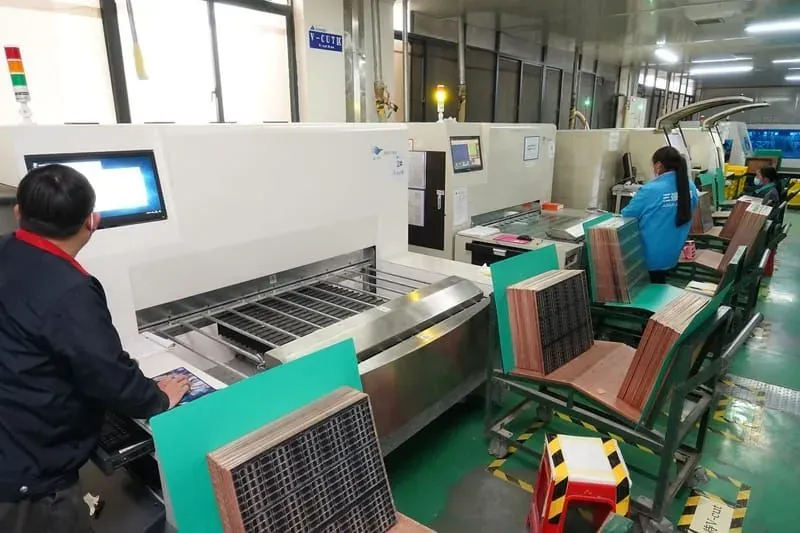
PCB Manufacturing Starts with Executable Data
A fabricator converts customer files into controlled production instructions. Gerber or other image data, drill files, stackup, finished thickness, copper requirements, impedance notes, outline, and surface finish must share one revision. This guide explains common process logic; the actual route and manufacturability require design-specific engineering confirmation.
Data Review and Engineering Preparation
The first review checks layer order, hole types, units, polarity, outline, solder-mask openings, and legend requirements. Engineering also identifies conflicting dimensions, spacing, or tolerances. Open issues should be clarified through questions rather than resolved by guessing design intent.
Inner-Layer Imaging and Inspection
For multilayer boards, inner layers commonly undergo image transfer, development, and etching before comparison with the production data. Material, copper requirement, and pattern density affect the process window. Compensation and control methods belong to the order-specific engineering plan and should not be presented as universal fixed values.
Treatment, Layup, and Lamination
Inner layers and dielectric materials are arranged to the approved stackup and laminated. Registration, resin flow, copper distribution, and material compatibility influence the result. Designers provide the target construction and critical electrical needs; manufacturing engineering confirms materials and the lamination route after review.
Drilling, Hole Preparation, and Metallization
Mechanical holes or other specified structures are produced from controlled data, followed by preparation for a clean, conductive hole wall. Hole structure, aspect relationship, material system, and reliability needs influence the suitable method. Special hole types must be clearly identified in RFQ files.
Outer-Layer Patterning, Copper Formation, and Etching
Outer circuitry is formed through image transfer, selective metal deposition, and etching. Line width, spacing, copper requirement, and panel distribution interact, so finished requirements belong in the drawing or order specification and feasibility must be confirmed by manufacturing engineering.
Solder Mask, Legend, and Surface Finish
Solder mask protects areas that should not remain exposed, legend carries assembly identification, and the pad finish is selected for assembly, storage, and product needs. Available materials, colors, finish choices, and standards remain subject to the project quotation and approved data.
Profiling, Electrical Test, and Final Inspection
Boards are profiled by routing, scoring, or another project-defined method, then receive order-defined electrical, dimensional, and visual checks. Special inspection, cross-sections, impedance records, or other reports should be requested during the RFQ and confirmed by engineering.
Connecting Fabrication to Assembly
If bare boards continue into PCBA, coordinate panelization, process edges, fiducials, surface finish, manufacturability, and revision control early. See the PCB assembly process guide and PCB assembly service. PCB168 confirms actual scope, schedule, quantity, and acceptance records only after reviewing the complete package.
Need PCBs for Your Project?
Get an instant quote — prototypes from $2, delivered worldwide.
Get Instant Quote