Is a 4 oz Copper PCB Standard or Heavy Copper? Where the Threshold Sits

You drew the board at 4 oz because the current budget said so. Now you are about to send it out, and a question you did not expect has become the most consequential one on the page: is this a standard PCB with thicker copper, or is it a heavy copper PCB?
It matters because the two are quoted off different capability tables. Not different prices for the same table — different tables. If you designed against the standard one and get quoted against the heavy copper one, the mismatch does not show up as a surcharge. It shows up as a feasibility question three days into the quote cycle, about a trace width you have already routed the whole board around.
The answer is a published number, and 4 oz is on the far side of it.
1. The threshold is 3 oz, and it is stated, not inferred
PCB168 defines heavy copper as 3 oz (105 µm) or more on inner and outer layers, against the 1–2 oz used on standard boards. That definition and the capability range attached to it are on the heavy copper PCB product page: copper weight 3 oz to 20 oz, 1 to 16 layers, board thickness 0.8 mm to 6.0 mm, minimum line width 6 mil, HASL / ENIG / OSP finishes, FR-4 TG170/TG180 material, impedance control ±10%.
So 4 oz is not near the threshold. It is one full step past it, and it is the lightest weight most people encounter *after* crossing. That position is why 4 oz generates more confusion than 8 oz does. At 8 oz nobody assumes they are on a standard board. At 4 oz it feels like a standard board with a heavier pour, and the number is small enough to keep that assumption alive right through layout.
There is a second reason the confusion survives: the general capability sheet lists copper weight as 0.5 oz to 20 oz in a single row. Read alone, that row says 4 oz is inside the standard envelope. It is inside the *company's* envelope. It is not inside the standard-board envelope, because the moment copper weight reaches 3 oz the process route changes and a different set of limits applies to everything else in that column. One row does not travel with the rest of its own table.
2. What "4 oz" describes, and the one ambiguity worth resolving early
Copper weight is an area-density unit carried over from foil supply: 1 oz of copper spread over one square foot, which works out to roughly 35 µm of thickness. 4 oz is therefore about 140 µm, and 3 oz about 105 µm — the figure the product page uses to anchor the heavy copper definition.
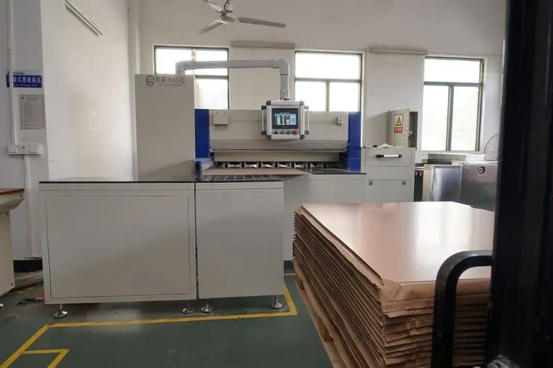
The picture at the top of this page is the reason the unit is expressed that way. Copper weight is a property of the laminate you start from, selected at material issue, not a thickness produced later in the process. A 4 oz board is not a standard board that received extra plating. It is a board cut from different stock, and every process step downstream inherits that choice.
Which raises the one ambiguity you should settle before quoting: does your 4 oz mean the base foil you specify on the laminate, or the finished copper after plating? On outer layers the two are not the same number, because plating adds copper on top of the foil. A 4 oz base foil on an outer layer finishes thicker than 4 oz. A 4 oz finished requirement on an outer layer starts from lighter foil.
Both readings are legitimate. Only one matches your current-carrying calculation. Resolving which basis you meant, and writing it down that way, is a separate piece of work covered in finished copper thickness versus base copper. For the threshold question, note only this: under either reading, a 4 oz outer layer is above 3 oz, so the classification does not change. The ambiguity affects what you get, not which table you are on.
3. Four published parameters move when you cross 3 oz
This is the part that makes the threshold worth knowing. The classification is not a label — it swaps the constraint set you should have been designing against.
| Parameter | Standard capability | Multi-layer PCB page | Heavy copper (3 oz+) |
|---|---|---|---|
| Min line width / spacing | 2 mil / 2 mil | 3 mil / 3 mil | 6 mil |
| Layer count | 1–40 layers | 4–40 layers | 1–16 layers |
| Board thickness | 0.2–6.0 mm | 0.4–6.0 mm | 0.8–6.0 mm |
| Impedance tolerance | ±5% (TDR verified) | ±8% | ±10% |
Standard and multilayer figures come from the capabilities page and the multi-layer PCB page; heavy copper figures from the heavy copper product page.
Three of the four tighten. One loosens in a direction that only helps if you were not counting on it. And they move together, as a set — which is the single most useful thing to understand about the threshold. You do not cross it for copper alone. You cross it and inherit three new ceilings at the same time.
4. Minimum line width is the one that breaks finished layouts
Of the four, the line width change is the one that turns a classification question into a re-layout.
Standard capability supports 2 mil / 2 mil. The multilayer product page states 3 mil / 3 mil. Heavy copper states 6 mil. If you laid out a 4 oz board against either of the lighter figures, the power geometry is almost certainly fine — heavy copper traces are wide by definition. The problem is everywhere else on the board.
A 4 oz design is rarely all power. It is a power stage plus the control circuitry that drives it: gate drive routing, a current sense pair, an I²C or SPI segment to a controller, maybe a small microcontroller footprint. Those nets were drawn at whatever width was comfortable. On a uniform 4 oz board they are now subject to the same 6 mil minimum as the power pours, because the constraint is a property of the copper thickness being etched, not of what the trace is carrying.
Why thickness sets the floor: etching removes copper from the sides of a trace as well as the top. The thicker the copper, the longer it stays in the etchant, and the more sidewall is lost. Suppliers compensate by widening the artwork, but compensation has a floor — below a certain width the feature cannot survive the etch with a usable cross-section regardless of how it was drawn. 6 mil is where that floor sits for this process window. The specific compensation and the width-versus-weight detail are covered in what copper weight does to trace width and spacing.
The practical consequence is a decision, not a fix. Either your fine geometry moves to 6 mil, or the board stops being uniformly 4 oz. The second option — thick copper on power layers, standard copper on signal layers — is a normal construction, and it is how most mixed-function power boards are actually built. It is also a different RFQ: you are specifying per-layer copper weights rather than one number for the board. The layer-count and weight-combination side of that is in thick copper multilayer layer count and copper weight limits.
What you should not do is send a uniform 4 oz board with 4 mil control traces and wait to see what happens. That is not a quote, it is a deferred feasibility review.
5. The layer ceiling and the thickness floor
Layer count drops from 1–40 to 1–16. For most 4 oz designs this is not binding; power boards tend to be 4 to 8 layers. It becomes binding in one specific case — when a design needs both high current and high interconnect density, and the layer count that satisfies the routing is above 16. At that point the two requirements are in direct conflict, and the resolution is usually mixed copper weights rather than uniform heavy copper, for the same reason as the line width problem.
Board thickness rises from a 0.2 mm floor to 0.8 mm. This is a physical consequence: copper occupies thickness. Four layers at 4 oz have roughly 560 µm of copper in the stack before any dielectric, and the dielectric between heavy copper layers must be thick enough to fill the space between features. A 0.8 mm floor is not a policy minimum, it is what the material adds up to. If you have a mechanical envelope specifying a thin board, check it against the floor before assuming the copper weight is the free variable.
Impedance tolerance widens from ±5% TDR-verified, or ±8% on multilayer, to ±10%. Wider trace geometry and thicker copper make controlled-impedance structures harder to hold. If your 4 oz board carries a controlled-impedance segment, ±10% is the tolerance that applies once the board is classified heavy copper — worth confirming against whatever your signal path was designed to, before it becomes an acceptance disagreement.
6. What this changes about the RFQ you are about to send
The threshold question has one operational answer: quote a 4 oz board as heavy copper, and state the copper weight basis explicitly.
Four lines, and the reason each one is there:
- Copper weight per layer, not per board. "4 oz" on a multilayer board is ambiguous about inner versus outer. State each layer, even if they are all the same. This is what lets the fab confirm the stack rather than assume it.
- Base foil or finished copper, stated. Say which basis your 4 oz refers to. Your current calculation depends on it, and the two numbers differ on outer layers.
- Minimum feature width actually present on the board. Not the minimum you would accept — the narrowest trace and gap in the design as drawn. If it is under 6 mil, that is the conversation to have first, and it is better to have it in the RFQ than in week two.
- Whether mixed copper weights are acceptable to you. If the answer is yes, say so. It opens a construction that may resolve the line width conflict without a re-layout, and the fab will not propose it unless it knows the option is open.
None of these are about price. They are about making sure the quote you receive is priced against the board you drew. That is the actual value of knowing where the threshold sits: not the classification itself, but that it tells you which table to check your own design against before anyone quotes it.
Copper weight, by the way, is not the input to derive first. Current and allowed temperature rise are — copper weight is what falls out of them. If 4 oz was chosen from a rule of thumb rather than a budget, deriving copper weight from current and rise covers that derivation, and it is worth doing before locking the number you are about to quote.
Ready to price it: request a heavy copper quote with your stackup and current requirements, or ask an engineer if the classification question is still open.
Related links
- Heavy Copper PCB capability and specifications
- Manufacturing capabilities overview
- Finished copper thickness vs base copper: what your 4oz callout means
- What copper weight does to trace width and spacing
- Thick copper multilayer: layer count and copper weight limits
- Deriving copper weight from current and temperature rise
---
FAQ
Is a 4 oz copper PCB a heavy copper PCB?
Yes. PCB168 defines heavy copper as 3 oz (105 µm) and above, so 4 oz is one step past the threshold and is quoted against the heavy copper capability set: 3–20 oz, 1–16 layers, 0.8–6.0 mm thickness, 6 mil minimum line width. It is not a standard board with a heavier pour.
How thick is 4 oz copper?
Roughly 140 µm, since 1 oz corresponds to about 35 µm. For reference, the 3 oz heavy copper threshold is stated as 105 µm on the product page.
Why does my minimum trace width change just because the copper is thicker?
Because etching attacks the sides of a trace as well as the top, and thicker copper spends longer in the etchant. More sidewall is lost, so a narrow feature cannot hold a usable cross-section. The published heavy copper minimum is 6 mil, against 2 mil / 2 mil standard and 3 mil / 3 mil on multilayer boards.
Does the 6 mil minimum apply to my control signals too, or only the power traces?
To everything on a layer built at that copper weight. The constraint follows the copper being etched, not the function of the net. If fine control geometry has to stay narrow, the usual answer is mixed copper weights — heavy copper on power layers, standard copper on signal layers — rather than a uniform 4 oz board.
Can I get a thin 4 oz board?
Not below the published 0.8 mm floor. Copper occupies thickness, and heavy copper layers need dielectric thick enough to fill between features. Check any thin mechanical envelope against that floor before treating copper weight as the free variable.
Does the 0.5 oz to 20 oz row on the capabilities page mean 4 oz is standard?
No. That row states the company's full copper range across all processes. Once copper weight reaches 3 oz the process route changes and the heavy copper limits apply to layer count, thickness, line width and impedance tolerance. A single row does not carry the rest of its own table with it.
Need PCBs for Your Project?
Get an instant quote — prototypes from $2, delivered worldwide.
Get Instant Quote