HDI PCB vs IC Substrate: Which One Is Your RFQ Actually For?

Two suppliers can look at the same set of Gerbers and come back with completely different questions. One asks for your stackup and impedance targets. The other asks for your die pad pitch and bump map. They are not being inconsistent — they have each classified your design differently, and that classification decides who quotes it, what data they need, and what language the acceptance clause is written in.
Getting this wrong is one of the quieter ways an HDI RFQ goes sideways. You are not comparing apples to apples, and you usually find out after the quotes arrive.
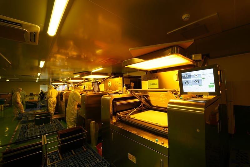
Why buyers put designs in the wrong bucket
The confusion is structural, not careless. High-end HDI and IC substrates share three of the same building blocks: laser-drilled microvias, any-layer interconnection, and very fine line width/space. Look at a cross-section and the family resemblance is real.
So the shorthand people fall back on is density. "It's really dense, so it must be a substrate." Density is not the dividing line. Plenty of demanding 14-layer any-layer boards are ordinary HDI work. Some very small, low-layer-count carriers are firmly substrate territory.
The functional distinction is simpler than the technical one. An IC substrate is the carrier that connects a bare semiconductor die to a PCB — it lives inside the package. An HDI PCB is the system board that the finished package gets soldered onto. If your design has a bare die landing directly on it with bump-level pitch, you are in substrate territory. If it receives packaged components, however fine their pitch, you are buying an HDI PCB.
That single question resolves most cases. The rest need the measurable checks below.
Three measurable features that actually decide it
1. Line width and space. This is the most useful single number. Our published HDI capability runs to 2mil/2mil (roughly 50µm) minimum line width and space, with 3/3mil listed as a standard fine-line feature. A design asking for conductors in that range is a fine-line HDI board. Designs that need conductors materially finer than what a fine-line PCB process holds have crossed into substrate process territory, which is a different equipment set and a different supplier conversation.
Practical use: pull the narrowest trace and tightest gap out of your design rules and compare them against the fab's published fine-line figure. If you are inside it, quote it as HDI. If you are asking for something well beyond it, say so explicitly in the RFQ rather than letting the fab discover it during DFM.
2. Microvia diameter and drill capability. Our HDI process laser-drills down to 0.075mm, with microvia diameters at 0.1mm and above. Those are PCB-scale microvias. Substrate-class via structures are a smaller order of magnitude and are built with different tooling.
Practical use: state your smallest via diameter and target aspect ratio as numbers in the RFQ. "Microvias" as a bare word tells a fab nothing about which process it needs to load.
3. Layer-to-layer registration. This is the feature buyers most often forget to specify and most often argue about later. We hold registration to ±25µm on HDI builds. Registration is what makes stacked and staggered any-layer interconnects manufacturable, and it is the constraint that tightens fastest as features shrink. Substrate-class work is held tighter still.
Practical use: if your annular ring budget assumes registration tighter than the fab's published figure, that assumption is the thing to surface first. It is far cheaper to discover it in the RFQ than in a first-article report.
Layer count and stackup are not the dividing line
This deserves its own heading because it is the most common false signal.
Our HDI capability spans 4 to 20 layers with 1+N+1 through 4+N+4 buildups. Every one of those is an HDI PCB. A 20-layer board with a 4+N+4 buildup is a demanding HDI job, not a substrate. Conversely, layer count alone tells a supplier almost nothing about process difficulty — an 8-layer any-layer board with 2mil lines is harder than a 16-layer board with 5mil lines.
So when you write the RFQ, lead with features, not layer count. Layer count belongs in the stackup attachment. The classification decision belongs to line width, via size, and registration. Our multi-layer PCB stackup guide covers how to express the stackup itself, and the PCB via design guide covers naming via structures unambiguously.
What the material choice tells the supplier
Material is a supporting signal rather than a decisive one, but it carries intent and it is worth getting right in the RFQ.
- FR-4 — the default for HDI system boards. If FR-4 meets your electrical and thermal needs, you are almost certainly in HDI territory and should quote it there.
- BT — chosen when you need better thermal and dimensional behaviour than standard FR-4. Common on higher-end HDI and on substrate-class carriers alike, so on its own it does not settle the category.
- ABF — associated with fine-line build-up construction and package-level carriers. Specifying ABF signals substrate-class intent, and a supplier will read it that way.
We build HDI on FR-4, BT and ABF, and we build IC substrate-class boards on ABF and BT for flip-chip, BGA and SiP packages. The overlap is exactly why material alone cannot classify your design — but naming your material in the RFQ removes a round of questions. If you are still choosing, high-frequency material selection is the place to start on the electrical side.
What you lose when the category is wrong
Misclassification does not usually produce an error message. It produces quotes that quietly do not answer your question.
Registration tolerance goes unstated. Standard PCB RFQ templates rarely have a field for layer-to-layer registration. On a design where annular ring is the binding constraint, leaving it blank means nobody has agreed to the one number that determines whether the board yields.
Acceptance language comes from the wrong standard family. A board quoted as a PCB gets inspected and accepted in PCB terms — IPC-6012 class levels, IPC-A-600 visual criteria. Package-level carriers are discussed in package-level terms. If your design genuinely sits at the boundary, you need to state which acceptance vocabulary the first-article report will use, because the two sets do not map cleanly onto each other.
You compare quotes across incompatible process groups. A fab quoting standard HDI and a supplier quoting substrate-class work will differ by far more than a normal competitive spread. Treating that gap as a negotiating position rather than a signal that the scopes differ is how buyers end up with a board that cannot be built to the assumptions they priced.
Assembly assumptions drift. If the board is going out for assembly, the classification affects what the assembler expects to receive and how they handle it. Worth aligning before the PCBA scope is fixed rather than after.
What to send for each category
Once you have decided, the data package differs. Send the right one and you skip a round trip.
For a high-end HDI PCB RFQ:
- Gerber or ODB++ with all layers, plus the drill files clearly separated by laser and mechanical.
- A stackup drawing naming every layer, dielectric, and copper weight, with symmetry shown.
- Minimum line width and space as explicit numbers, not just design-rule files.
- Via structure by type: through, blind, buried, stacked, staggered — with diameter and depth for each.
- Impedance requirements with tolerance, and which layers they apply to.
- Layer-to-layer registration requirement, or a statement that the fab's standard applies.
- Board thickness and thickness tolerance, plus finished outline.
- Surface finish and any selective finish areas.
- Acceptance standard and class level.
- Quantity split between prototype and production, so tooling can be amortised sensibly.
For a substrate-class carrier RFQ, add or change:
- Die attach method and whether a bare die lands on the carrier.
- Pad pitch and pad geometry at the die interface.
- Bump or pillar details if flip-chip.
- Package outline and how the carrier integrates into it.
- The acceptance vocabulary you expect, since PCB visual standards may not cover the features that matter.
- Any singulation or handling requirements specific to package assembly.
If you genuinely do not know which list applies, send the first one and flag the die-attach question at the top of the email. A supplier can reclassify from a complete HDI package far more easily than from an incomplete substrate package.
Four things to get engineering to confirm before the PO
None of these should be assumed from a capability table, including ours. Capability figures describe what a process can reach under the right conditions — not that your specific combination of features is buildable together at the price you were quoted.
- That your narrowest line and tightest space are achievable together with your via structure on your chosen material. Each is fine alone. The combination is the question.
- That your annular ring budget survives the actual registration tolerance being offered. Ask for the number in writing, applied to your stackup.
- That your smallest via diameter is achievable at your board thickness and aspect ratio. Via size and board thickness constrain each other.
- Which acceptance standard and class the first-article report will be written against, and that both sides read the boundary features the same way.
Get these four in writing and the rest of the RFQ is ordinary commercial work. Skip them and you have priced an assumption. You can send the design through our quote form or raise the boundary question directly with engineering via contact; the HDI PCB capability page lists the published figures referenced above, and the HDI manufacturing process guide walks the build sequence if you want context on why registration behaves the way it does.
FAQ
Is an IC substrate just a very dense PCB?
Functionally no. An IC substrate is the carrier that connects a bare semiconductor die to a PCB and sits inside the package. An HDI PCB is the system board the finished package mounts to. They share process building blocks — laser microvias, any-layer interconnection, fine lines — but they occupy different positions in the assembly.
My design has 2mil lines and stacked microvias. Is that a substrate?
No. 2mil/2mil with stacked microvias is within our published fine-line HDI capability. Quote it as an HDI PCB and state the features explicitly.
Does a high layer count push my design toward substrate class?
No. We build HDI from 4 to 20 layers with 1+N+1 to 4+N+4 buildups, all of it HDI. Layer count affects difficulty and cost, not category.
What single question settles it fastest?
Does a bare die land directly on this board? If yes, you are in substrate territory. If it receives packaged parts, however fine the pitch, you are buying an HDI PCB.
Should I specify registration tolerance in my RFQ?
Yes, whenever annular ring is a binding constraint. We hold ±25µm on HDI builds; if your design assumes tighter, that is the first thing to raise rather than the last.
What if my design sits right on the boundary?
Send the line width, via structure and pad pitch and ask for a classification before quoting. That call is cheap at the RFQ stage and expensive after tooling.
Does the category change what my assembler needs?
It can. Handling, singulation and acceptance expectations differ at the package level, so align the classification before you fix assembly scope.
---
Need PCBs for Your Project?
Get an instant quote — prototypes from $2, delivered worldwide.
Get Instant Quote