PCB Design Services Outsourcing for HDI Boards: Who Owns DFM
The mismatch that produces double rework
An outsourced HDI project has three parties, and each one holds information the other two do not:
- You own the requirement: what the board has to do, what it has to fit inside, what it costs to be late.
- The design house owns the layout: placement, routing, constraint closure, and the CAD database itself.
- The fabricator owns the process: what its actual line can hold, which stackups it laminates repeatably, which via structures it drills and plates without a feasibility caveat.
The classic sequence is that parties one and two complete a full design cycle before party three is asked anything. The design house picks a stackup that is defensible in the abstract — a symmetric build, a sensible dielectric arrangement, a via structure that matches the textbook — and routes the whole board against it. Then the files reach a fabricator, who reads the stackup and says: we would build this differently.
At that point the cost is asymmetric and badly distributed. Changing the stackup after routing is not a stackup change. It is a re-route, because layer assignment, impedance-controlled trace geometry and via transitions were all derived from the stackup that just moved. You pay the design house again for work that was correct when it was done.
The inverse failure is quieter and worse. The fabricator accepts the files as drawn, absorbs the difficulty silently, and the board becomes harder to build than it needed to be. You do not see a quote revision. You see it later, in yield conversations you were not expecting, on a board whose design nobody wants to reopen.
Both failures come from the same root cause: the stackup and via structure were decided by whoever happened to reach them first, rather than by whoever owns the process that has to realise them.
Decision rights: the split that actually holds
The useful question is not "who is responsible for DFM." Everyone answers yes to that and nothing changes. The useful question is *who has the final call on each specific decision, and who has to be consulted before it is made.*
| Decision | Final call | Must be consulted before it is fixed |
|---|---|---|
| Functional requirement, mechanical envelope, connector positions | You | Design house (routability), fabricator (only if envelope forces board thickness) |
| Component selection and pin pitch | You | Design house — pitch drives the routing density that drives everything downstream |
| Layer count | You, on the design house's recommendation | Fabricator — layer count interacts with thickness and copper weight |
| Stackup: dielectric arrangement, core/prepreg choice, copper distribution | Fabricator | Design house — it has to route against the result |
| Via structure: microvia levels, blind/buried arrangement, via-in-pad treatment | Fabricator | Design house — via strategy sets escape routing |
| Impedance-controlled trace geometry | Design house, against the fabricator's confirmed stackup | Fabricator, if the target cannot be met in the confirmed build |
| Placement and routing | Design house | You, for serviceability and test access |
| Minimum feature sizes actually used | Design house, inside the fabricator's confirmed window | Fabricator, if the design needs to go below the standard fine-line grade |
| Surface finish | You, on both parties' input | Fabricator — finish interacts with fine-pitch pad geometry |
| Acceptance criteria and test coverage | You | Fabricator, for what is verifiable at panel level |
| Any change after stackup confirmation | You, in writing | Both |
Two rows in that table are the whole article. Stackup and via structure sit with the fabricator, and everything the design house does afterwards is downstream of them. Get those two rows agreed before kickoff and most of the rework disappears.
Note what the table does not say. It does not say the fabricator designs your board, or that the design house is a subordinate. It says each party has final authority where it owns the physical reality — and that authority is exercised *before* the dependent work starts, not after.
Why stackup and via structure cannot be outsourced with the layout
Three reasons, and they are independent of any particular supplier.
A stackup is a process output, not a drawing. The published capability window at PCB168 — 1–40 layers, 2mil/2mil minimum line width and space, 0.075mm laser drilling, 0.2–6.0mm board thickness — describes what the line can hold. Which specific dielectric arrangement lands inside that window for *your* layer count, copper distribution and finished thickness is a build decision. A design house working from published numbers can produce something plausible. Only the party that laminates it can confirm it is repeatable.
Via structure is bounded by stackup, and escape routing is bounded by via structure. HDI builds at PCB168 run 1+N+1 up to 4+N+4, with blind and buried vias and via-in-pad filled and capped. Those are different escape-routing problems. A 1+N+1 gives you one microvia level per side; a 2+N+2 gives you two, and lets a dense BGA breathe in ways a 1+N+1 cannot. If the design house assumes two levels and the confirmed build has one, the escape pattern under every fine-pitch device is wrong. That is not a correction. That is a re-route. Our via design types guide covers what each structure buys you before you commit to one.
Impedance is derived, not specified. A design house cannot hit an impedance target against a stackup that has not been confirmed, because trace geometry is solved *inside* a known dielectric arrangement. Specifying "50 ohm" and letting the layout proceed against an assumed build means the geometry gets re-solved when the real build arrives — and the traces move. The multi-layer stackup guide shows the dependency chain in the order it actually runs.
The practical rule that falls out of all three: the fabricator confirms the stackup and via structure before the design house starts routing, not after it finishes. One confirmation cycle at the start, on a document, costs a fraction of one re-route cycle at the end, on a database.
Deliverables and file ownership
Ambiguous file ownership is the second-largest source of avoidable friction, and it surfaces at the worst possible moment — when you want a second quote, or when the design house is no longer available.
Settle these before kickoff, in writing:
What you receive at the end of the engagement. Not just the manufacturing outputs. The native CAD database, the constraint and rule set, the library entries for every part used, and the schematic in an editable form. Manufacturing outputs alone — Gerbers, drill files, netlist, assembly drawings — let you build this revision at this fabricator. They do not let you make revision B, and they do not let you move the board somewhere else without a re-import that loses intent.
Who holds the constraint set. The constraints encode why the layout looks the way it does. If they live only inside the design house's tool, the reasoning leaves with the engagement. Require them as a delivered artefact, not a screenshot.
Library provenance. Footprints built for this project should arrive with the pad geometry rationale attached, particularly for fine-pitch parts and any BGA. Fine-pitch pad geometry interacts with surface finish and with the minimum feature window; a footprint that was fine in isolation can be the reason a build needs a caveat.
The stackup document, as confirmed. This is a jointly owned artefact. It is the record of what the fabricator confirmed and what the design house routed against. When something is questioned six months later, this document is the only thing that settles who agreed to what. Keep it versioned and keep it out of email.
Fabrication notes authorship. Notes drive how the fabricator interprets everything else — tolerance intent, acceptance criteria, what is critical and what is nominal. Decide explicitly whether the design house writes them, whether you review them, and who has final wording. Vague notes are how "the drawing said so" arguments start.
The change approval chain
After the stackup is confirmed, changes stop being local. This is the part most engagements never write down, and it is where the double-rework loop closes.
Every change gets classified before it gets implemented. Three classes:
- Class 1 — layout-local. A trace re-route inside a confirmed stackup, a silkscreen fix, a refdes correction. Design house implements, notifies. No fabricator involvement.
- Class 2 — touches the build. Layer count, thickness, copper weight, via structure, minimum feature sizes, anything that moves the stackup. Fabricator confirms *before* the design house implements. Non-negotiable ordering.
- Class 3 — touches requirements. Component swaps that change pitch or footprint, connector moves, envelope changes. You approve, then it flows through Class 2 if it touches the build, then Class 1.
Class 2 has one direction and no shortcut. Confirm, then implement. The reverse order — implement, then ask — is exactly the sequence that produces the re-route you are trying to avoid. The whole point of writing the chain down is that under schedule pressure, the reverse order feels faster.
Every change carries an impact statement. One or two lines: what moved, what else it touches, whether the build changed. Not a form. A note in the change record that the next person can read.
One named approver per party. Three people, named at kickoff. Not roles, not distribution lists. Named. A change record that ends in "the team agreed" is a change record that will be disputed.
Nothing is approved in a chat thread. Chat is where the discussion happens. The decision lands in the change record, or it did not happen. This costs a few minutes per change and saves the argument about whether a message counted as approval.
Three things to write into the contract or PO before kickoff
If the rest of this article is too much to negotiate, these three lines carry most of the value.
One. The stackup and via structure are confirmed by the fabricator before routing starts, and confirmation is a document. Name the artefact and make it a milestone with a date. Routing does not begin until it is signed. This single clause removes the largest rework path in the engagement.
Two. You receive the native CAD database, the constraint set and the libraries, not only manufacturing outputs. State the file formats. "Native design files" is not a specification — a design house and a customer can hold genuinely different beliefs about what that phrase includes, and both can be sincere.
Three. Changes touching the build require fabricator confirmation before implementation, with one named approver per party. Write the three names into the kickoff record. If a name changes mid-project, that is an update to the record, not an informal handover.
Everything else — review cadence, DFM check timing, who runs which verification — can be negotiated as you go. These three cannot, because each one is load-bearing for work that starts immediately.
What is quotable at kickoff and what needs engineering review
An honest split, because "we'll figure it out" is where schedules go to die:
Confirmable early, from the published capability window: whether your layer count is in range; whether your finished thickness is in range; whether your minimum feature sizes are inside the fine-line window; whether your via structure family is supported; whether your surface finish is available; whether blind/buried vias and via-in-pad are on the table at all.
Needs engineering review before anyone commits: the specific dielectric arrangement for your layer count and copper distribution; whether your impedance targets are achievable in that arrangement; whether the escape routing under your densest device works in the confirmed via structure; whether a design that needs to go below the standard fine-line grade can hold it in your particular build; and any combination that sits near more than one published edge at once.
The second list is not a delay. It is the list that, if skipped, becomes a re-route. Send the mechanical envelope, the layer count, the densest device's pitch and package, your impedance targets and the finished thickness through our quote route, and the review happens against real constraints instead of assumptions. The HDI PCB page has the current window, and the HDI manufacturing process article explains why the build sequence constrains the design in the order it does.
FAQ
Can I outsource HDI layout without involving a fabricator until the design is finished?
You can, and the design will usually be competent. But the stackup and via structure will have been assumed rather than confirmed, and if the assumption misses, the correction is a re-route rather than an edit. One confirmation cycle before routing starts is cheaper than one re-route after it finishes.
Who is responsible if an outsourced HDI design turns out to be hard to manufacture?
Responsibility follows decision rights, which is exactly why they need to be written down. If the fabricator confirmed the stackup and via structure and the design house routed inside that confirmation, difficulty is a process question. If the design house chose a build the fabricator never saw, it is a design question. Without a documented split, it becomes an argument, and arguments do not ship boards.
What files should I insist on receiving from a design house?
The native CAD database, the constraint and rule set, the project libraries with footprint rationale for fine-pitch parts, the editable schematic, the confirmed stackup document, and the manufacturing outputs. Manufacturing outputs alone build this revision at this supplier — they do not give you revision B or a second source.
Should the design house or the fabricator run the DFM check?
Both, at different points and for different things. The design house checks its own rule closure continuously. The fabricator checks against its actual process, and that check is only meaningful against a confirmed stackup. Sequence matters more than ownership: confirm the build, route against it, then verify.
Does the fabricator confirming the stackup mean I am locked to that supplier?
Not if you hold the native files, the constraint set and the confirmed stackup document. Those three make the design portable. What is not portable is a layout whose build assumptions were never recorded — that one is locked to whoever happened to interpret it, whether you intended that or not.
Sources: PCB168 deployed capability page (layer count, minimum line width/space, drilling, board thickness, copper weight, HDI stackup range, microvia diameter, layer-to-layer registration, blind/buried via and via-in-pad support), PCB168 deployed HDI PCB product page, PCB168 deployed multi-layer PCB product page. Standards referenced by name only: IPC-2226 (HDI design), IPC-2221 (generic printed board design), IPC-6012 (rigid printed board performance). No claim in this article asserts a PCB168 yield, lead time, price, capacity, certification, customer case, design-service offering or numerical DFM rule beyond the published capability pages.
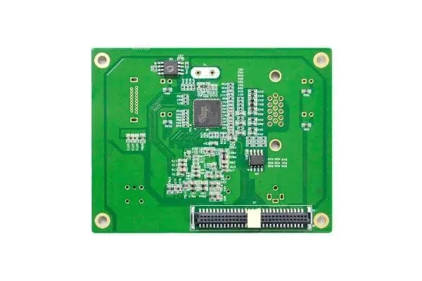
Image alt: Populated compact green printed circuit board photographed straight down on a white background, showing a fine-pitch square IC at centre, a grid of round gold-plated pads at upper right, a high-density two-row board-to-board connector along the bottom edge, and gold-ringed corner mounting holes.
---
Related links

Need PCBs for Your Project?
Get an instant quote — prototypes from $2, delivered worldwide.
Get Instant Quote