Heavy Copper PCB, Busbar or Copper Inlay: Choosing the High-Current Carrier
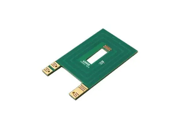

You have a number. Maybe it is 60 A continuous into a motor drive, maybe 150 A peak out of an inverter leg. The number is settled, the topology is settled, and you are now stuck on something that no current-capacity table will answer: should this current be carried by the board, by a busbar bolted outside the board, or by a copper slug inlaid into just the part of the board that needs it?
All three can reach your amp target. That is precisely why the amp target cannot choose between them. Ask a supplier "what copper weight do I need for 100 A" and you will get a useful answer about copper cross-section — and you will still not know whether the copper belongs in the laminate at all.
Three other questions decide it. This page walks each one, then says which of the three carriers you can actually quote against a published capability table today, and which two need a feasibility conversation before anyone talks price.
1. Why the amp target is the wrong starting point
Current capacity is a function of copper cross-section and allowed temperature rise. Cross-section is width times thickness. So for any target you can trade width against thickness fairly freely, and each of the three carriers is just a different point on that trade:
- Heavy copper PCB — thickness goes up across the whole layer, so every conductor on that layer gets wide-and-thick capability whether it needs it or not.
- Busbar — the cross-section leaves the laminate entirely and becomes a solid bar sized independently of anything on the board.
- Copper inlay — thickness goes up only inside a defined region, leaving the rest of the layer at normal weight.
Each of those reaches the same number. What differs is what else changes as a side effect, and side effects are what you are actually choosing between. A decision framed as "how many amps" collapses into a copper-weight question and hides the three constraints that matter.
2. Question one: how far does the current travel inside the board?
Distance is the first separator, because copper cross-section costs money per unit length and each carrier prices length differently.
Short runs — the current enters, crosses a few centimetres to a switching device or a shunt, and leaves. Here the heavy copper region is a small fraction of the board area. Thickening the entire layer to serve it means paying heavy copper economics across a board that is mostly not carrying power. This is the case where a localised approach looks attractive, and where an inlay is the concept that fits, if it is feasible at all.
Medium runs across most of the board — power enters at one edge, distributes through planes, feeds several stages, exits at another edge. Now the thick region *is* the board. Thickening the whole layer is not overkill, it is the efficient answer, and a heavy copper build is the natural fit. This is the majority case in power supply PCBs and it is why heavy copper exists as a standard product category rather than a special request.
Long runs, or runs between boards — the current has to get from a rectifier assembly to an inverter assembly, or from a battery interface to a distribution point, and the path is longer than the board is. Trying to make the laminate do this means a board that exists mostly to be a conductor. A bar does it with less material, less area and no laminate in the path at all.
One nuance that trips people: distance means *electrical path length*, not board dimension. A 300 mm board where power enters and exits on the same edge may have a 60 mm path. Measure the path, not the outline.
3. Question two: does the path have to be serviceable?
This question has only two answers and it is the fastest of the three to resolve, so ask it early.
A conductor etched into laminate is permanent. You cannot unbolt it, you cannot swap it after a fault, you cannot re-torque it in the field, and you cannot reconfigure the distribution without a new board. For most power supplies that is fine — nobody services a power plane.
But some designs genuinely require a demountable joint: modules that get replaced as units, distribution that gets reconfigured between product variants, connections that must be inspected or re-torqued on a maintenance schedule, or interfaces where a field technician has to disconnect power before servicing something else. A bolted bar gives you that. Etched copper cannot.
Be honest about the answer, because "serviceable" carries a cost. Every demountable joint is a mechanical interface: contact area, contact pressure, plating at the mating face, thermal cycling of a bolted assembly, and a torque spec that someone has to actually follow. You are trading a permanent low-risk connection for a serviceable connection that needs specification and control. If nothing in your product lifecycle requires the joint to open, you are buying a liability.
Note what this question is *not*. It is not about how power gets into the board — that is an interface question, and terminals, press-fit and via arrays are all covered in the connection interface RFQ inputs. This question is about whether the *distribution path itself* has to come apart.
4. Question three: how much fine routing shares the board?
This is usually the decider, and it is the one most often discovered too late.
PCB168 publishes a minimum line width of 6 mil for heavy copper builds, against much finer geometry available on standard boards. That minimum is a process consequence: thick copper undercuts during etching, so the etch compensation needed to land a thick conductor at its target width sets a floor on how narrow anything on that layer can be.
Which means the choice is not only about your power conductors. Thickening a layer applies the 6 mil floor to everything else on that layer. If your power stage shares a board with a microcontroller, a gate driver with tight feedback routing, a fine-pitch package, or an analogue sense path that wants controlled geometry, the heavy copper window may not have room for them on the same layer.
Three ways out, in order of how much they cost you:
- Separate the layers. Heavy copper is available on 1–16 layers, so power layers can carry the thick copper while signal layers stay at normal weight. This is the standard resolution and it is why the multilayer mixed-weight case has its own stackup declaration.
- Separate the boards. Power board plus control board, with an interconnect between them. Costs an assembly interface, buys complete freedom on both sides.
- Keep the layer thin and move the copper off-board or into a local region. This is where busbar and inlay come back into consideration — not because they carry current better, but because they leave the layer's geometry alone.
If option 1 works, take it. It stays inside a published capability window. The other two are architectural decisions with their own cost.
5. What is quotable today, and what needs a feasibility check first
This is the practical asymmetry, and ignoring it is how a schedule slips.
Heavy copper PCB — quotable against a published table. The heavy copper PCB page states the window: copper weight 3 oz to 20 oz, 1 to 16 layers, board thickness 0.8 mm to 6.0 mm, minimum line width 6 mil, HASL / ENIG / OSP surface finish, FR-4 TG170/TG180 material, impedance control ±10%. If your design sits inside that, you can send files and get a quote through the normal cycle.
Busbar — a mechanical part, not a PCB line item. A bar is outside the board. It has its own material spec, its own plating, its own fabrication and its own mounting hardware, and it is procured as a mechanical component. What lands on the PCB side is the interface: pads, mask openings, hole sizes, finish at the contact face. So a busbar decision does not simplify your PCB spec — it splits your bill of materials and adds a mechanical drawing, while leaving you a PCB interface to specify anyway.
Copper inlay — not in the published window; confirm before you design around it. Embedding a thicker copper element into a defined region is a different process family from thickening a layer, and it is not part of the published heavy copper capability above. Treat it as something to confirm as feasible, with its own inputs and its own acceptance criteria, before it appears in your stackup. Designing a board around a process you have not confirmed is the expensive version of this mistake.
The asymmetry has a practical consequence for sequencing: if heavy copper can solve your problem, resolving it there costs you a normal quote cycle. The other two cost you a feasibility exchange first. That is not a reason to rule them out — sometimes they are the right answer — but it is a reason to test the heavy copper path before assuming you need something else.
6. Running the three questions in order
The questions are not independent and they are not equally decisive. Run them in this order, because each one can end the decision:
Start with serviceability. If the joint must be demountable, you need a mechanical interface, and that pushes you toward a bar for the demountable segment regardless of the other answers. If it does not, drop the bar from consideration for the *distribution path* and move on.
Then check fine routing. If the same layer must carry both high current and geometry finer than 6 mil, and layer separation cannot resolve it, the layer cannot be thickened. That is a hard constraint, not a preference, and it forces you off the whole-layer approach.
Then look at distance. With the first two answered, distance tells you whether whole-layer thickening is efficient or wasteful. Most of the board carrying power means heavy copper. A small fraction means the localised approach is worth a feasibility question.
A worked example of the ordering: 80 A continuous, path about 50 mm, no serviceability requirement, and a gate driver with fine feedback routing on the same board. Serviceability says no bar. Fine routing says the signal geometry cannot share a thickened layer — but layer separation resolves it, because heavy copper supports up to 16 layers. Distance says 50 mm on a small board is most of the path. Answer: multilayer heavy copper with the power on thick layers and the driver routing on a normal-weight layer. It sits inside a published window and needs no feasibility exchange. The inlay question never had to be asked.
Change one input — make the joint serviceable — and the bar comes back for that segment while the board still handles distribution. Change a different one — make the thick region 10% of a large board — and inlay feasibility becomes worth asking about.
7. What to put in the RFQ once the carrier is chosen
Whichever carrier you land on, state the decision and its basis. A supplier who can see why you chose it can tell you when the choice does not hold.
Five lines cover it:
- The carrier decision and its reason — "whole-layer heavy copper, path is most of the board, no serviceable joint required."
- The electrical path, described as a route: where current enters, where it exits, what it passes through, and the approximate path length.
- Continuous and peak current separately, with duty cycle. If these drive your copper weight, the thermal budget approach is the piece that turns them into a weight.
- The finest geometry that must coexist, and on which layer. This is what tells the supplier whether the 6 mil floor is a problem.
- Whether any joint must be demountable, and if so, which one and why.
If you are choosing between quotes rather than building one RFQ, note that carrier choice changes what the quote comparison is even comparing — a whole-layer quote and a mixed-stackup quote are not the same scope.
And if the answer turns out to be whole-layer heavy copper inside the published window, you can move straight to files: request a quote.
Related links
- Heavy Copper PCB capability window — the published table your design has to sit inside
- High-current connection interface RFQ inputs — what to specify at each interface once the carrier is set
- Copper weight from current and thermal budget — turning amps and temperature rise into a weight
- Mixed copper weight multilayer stackup — how to declare thick power layers beside normal signal layers
- Request a quote
---
FAQ
Is a busbar always cheaper than heavy copper for high current?
No, and the comparison is not like-for-like. A bar removes copper from the laminate but adds a mechanical part, its plating spec, its mounting hardware and a PCB interface you still have to specify. It tends to win on long paths and when a demountable joint is required. On a path that is mostly inside a single board, it adds parts and interfaces without removing the board.
Can I use heavy copper on only part of a layer?
Partial thickening within one layer is not the same as whole-layer heavy copper, and it is not part of the published capability window. The supported way to mix weights is across layers, not within one. If the localised approach is what your design needs, raise it as a feasibility question before you commit the stackup.
Does the 6 mil minimum line width apply to my whole board or just the thick layer?
It is a property of the thickened layer, which is why mixed stackups exist. Signal layers at normal weight keep their own geometry window. What you cannot do is put fine routing and heavy copper on the same layer and expect both. Declare which layers carry which, so the constraint lands where you intend.
My current target is high but the path is short. Is that automatically an inlay case?
It makes inlay worth asking about, not automatically correct. Check two things first: whether whole-layer thickening on a multilayer build is acceptable in cost terms, and whether the fine routing on the board can move to its own layer. If both work, you stay inside a published window with no feasibility exchange. Inlay becomes interesting when the thick region is a small fraction of a board you cannot afford to thicken entirely.
Can a single design use more than one carrier?
Yes, and it is common on larger systems. A bar handles the long demountable segment between assemblies, while heavy copper handles distribution inside each board. Split the path into segments, answer the three questions per segment, and specify each interface where segments meet. Do not force one carrier across the whole path because it won on one segment.
Need PCBs for Your Project?
Get an instant quote — prototypes from $2, delivered worldwide.
Get Instant Quote