HDI PCB Surface Finish: What to Declare for Fine-Pitch and Via-in-Pad
The finish options you copied came from the wrong table
Worth putting the two tables next to each other, because the gap is the whole problem.
Table on /capabilities/ | Rows that bear on this decision |
|---|---|
| Standard PCB | Min line width/space 2mil/2mil · min drill 0.1mm mechanical, 0.075mm laser · copper weight 0.5oz–20oz · Surface finish: HASL, ENIG, OSP, immersion tin/silver |
| HDI PCB | Stackup 1+N+1 to 4+N+4 · microvia diameter ≥0.075mm · layer-to-layer registration ±25µm · min line width 2mil · blind/buried vias yes · Via-in-Pad: filled and capped |
Read the HDI row set on its own and it tells you something the standard row set never does. The HDI table's answer to "what happens at the pad" is not a finish name. It is a *structural* statement: via-in-pad is filled and capped. The finish is what goes on top of that cap, and the cap is not the same surface as a plain copper pad.
So the sequence a buyer needs is the reverse of the one the page layout suggests:
- What is the finest pitch on the board, and what package type sits at that pitch?
- Is there via-in-pad under any of those pads? On an HDI build with an any-layer or stacked structure the answer is usually yes.
- Given 1 and 2, what does the pad surface look like before finish — flat, slightly dished, slightly proud?
- *Then* choose the finish, and declare the condition it has to hold rather than just its name.
Step 4 is where most RFQs start. Steps 1 through 3 are the ones that make step 4 answerable.
One more reason this ordering matters on HDI specifically: the product page builds these on FR-4, BT or ABF, across 4 to 20 layers, with registration held to ±25µm. Those are three independent variables that all touch pad flatness. A finish declaration that ignores them is a declaration about chemistry only.
Fine pitch constrains the finish; preference does not
Here is the sentence that changes how the line gets written: as pitch falls, the finish stops being a preference and becomes a dimensional requirement.
A finish does two jobs. It keeps copper solderable until assembly, and it presents a surface the paste and the reflow profile can work with. At 1.27mm pitch on a 2-layer board, job two is trivially satisfied by anything. Nobody is measuring the finish as a dimension, because the pad is large, the paste deposit is large, and the tolerance stack has room in it.
At 0.4mm pitch the pads are small, the paste deposits are small, and the stack has almost no room. Now the same finish participates in the tolerance chain three ways:
- It adds a layer. Whatever the finish's own build-up is, it sits on top of the pad and becomes part of the height each ball has to bridge.
- It varies pad to pad. No process deposits perfectly uniformly across a panel. At large pitch the variation is noise; at fine pitch it is a fraction of the gap you have.
- It determines what the pad looks like topographically. Some finishes are essentially conformal to whatever was underneath. Some level the surface. This is the difference between a finish that hides a slightly dished pad and one that faithfully reproduces it.
That third point is why the finish question and the via-in-pad question cannot be answered separately, and it is the part almost no RFQ addresses.
Notice what is deliberately absent from the list above: numbers. No coating thickness in µin, no coplanarity tolerance in µm, no pitch-to-finish limit table. We will not publish those here, because PCB168 has not published them as capability values, and an invented number in a buyer guide becomes a spec someone quotes back at a supplier. The capabilities page publishes registration at ±25µm and impedance at ±5% TDR-verified; it does not publish a finish thickness window, so neither will this article. What the article can do is tell you which conditions to *ask* to have written down.
Practically, the pitch-driven questions to put in the RFQ are:
- The finest pitch on the board, stated as a number, with the package type at that pitch (BGA, CSP, QFN, 0201 passives, or a mix).
- Whether any fine-pitch field sits over via-in-pad.
- Whether the board carries both fine-pitch and larger, heavier features on the same side, because that is a competing requirement inside one finish selection.
- Whether the assembler has a finish they require or refuse, which is a separate input from what you would pick.
Send that with the stackup and file set described in the HDI quote package checklist, and the finish line stops being a guess on either side.
Filled and capped: the surface the finish has to sit on
Via-in-Pad: filled and capped is one row in the HDI table, and it carries more consequence for the finish line than anything else on the page.
Break the phrase apart. A microvia lands inside a component pad rather than beside it. Left open, that hole would swallow paste during reflow and starve the joint. So the via is filled — the hole is closed with a fill material — and then capped — plated over so the pad reads as a continuous conductive surface again. The board then goes to finish.
Which means, on a via-in-pad HDI board, the finish is not being applied to a plain copper pad. It is being applied to a pad whose centre region was recently a hole, was filled, and was plated closed. Three independent processes contributed to that surface before the finish chemistry ever touched it.
Two things follow, and both belong in the RFQ.
First, flatness at the pad is a declared requirement, not an assumption. A capped via can finish flush with the surrounding pad, or it can end slightly dished, or slightly proud. Which one you get is a process outcome, and the acceptable condition is something you state and the supplier confirms — not something you infer from the word "capped". Ours is published as filled and capped; the *condition of the cap surface your assembly needs* is still yours to specify. Say what has to be true at the pad, and ask how it is verified.
Second, the verification of fill and the verification of the finish are different checks. The capabilities page lists X-ray inspection covering BGA and via fill verification, and cross-section microsection for quality validation. X-ray looks through the board at whether the fill is there and sound. Neither of those is a statement about the finished pad's outer surface. If your build needs both confirmed, ask for both, and ask what record you receive for each.
This is also the clean boundary with the microvia article. The stacked and staggered microvia declaration is about the via *structure* — where columns land, which layers they span, why the choice between stacked and staggered changes the build. This article starts one step later, at the moment that structure surfaces inside a pad and has to be handed to assembly. Same feature, different field, and you need both declared.
A useful way to phrase it internally: the microvia declaration tells the fabricator what to build. The finish declaration tells them what to hand over.
Where a weak finish line surfaces: at SMT, not at incoming inspection
This is the part that makes an under-specified finish line expensive rather than merely untidy.
Incoming inspection checks the board against the drawing. Dimensions, layer count, hole sizes, mask, markings, electrical continuity, the finish *named* as correct. If the RFQ said ENIG and the board arrived with ENIG, the finish field passes. Every box on the receiving checklist gets ticked. The board is booked into stock as conforming.
Nothing in that sequence tests whether the finish, on this particular pad topography, at this particular pitch, will produce good joints. That question is only answered when paste goes down and the board goes through reflow.
So the failure mode is not "bad board rejected at receiving". It is:
- Board passes incoming inspection.
- Board is released to assembly, often with components already bought against it.
- Fine-pitch joints come out inconsistent — some fields fine, some fields not.
- Diagnosis begins, and it begins in the wrong place, because the visible symptom is a solder joint and solder joints have many causes. Paste, stencil, profile, placement, and board surface are all candidates. Our solder joint failure article walks that diagnostic tree.
- If it does trace back to pad condition or finish, the board is still *conforming to its own drawing*. There is no non-conformance to raise, because the drawing never stated the condition that was actually needed.
Step 5 is the one worth sitting with. An under-specified finish line does not produce a supplier failure. It produces a board that is simultaneously correct and unusable, with no contractual route to a remedy. The cost lands as scrap, rework, schedule, and an argument nobody can win on paper.
The fix is entirely upstream and costs nothing at RFQ stage: state the condition, not just the name. Name the finish, state what has to be true at the pad, state how it is confirmed, and state what record comes with the shipment. Then a shortfall is a real non-conformance instead of a disagreement.
One related trap, since it shows up on the same line: a quote that comes back notably cheap on an HDI build has usually made assumptions somewhere, and finish plus pad condition is a common place for them to hide. The cheap HDI quote assumption check covers how to read that back.
Solderability life and reflow count belong in the declaration
Two more items ride on the finish line, and both get left off because they feel like someone else's problem.
Solderability has a shelf life. A finish protects copper from oxidation for a period, under storage conditions, and that period ends. Different finishes behave differently here — some are robust for a long time, some are more sensitive to time and handling. Our finish comparison covers the relative characteristics. What matters at RFQ stage is the consequence: if your boards will sit in stock before assembly, or ship to an assembler on a different schedule, the storage and shelf-life expectation is part of the order, not a detail to sort out later.
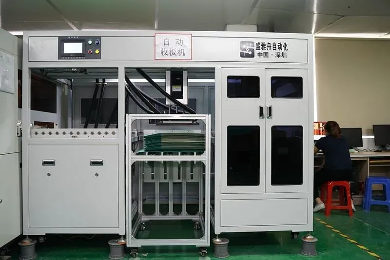
This is where the cover image on this article comes from, and why it is a handling shot rather than a board shot. Finished bare boards stacked on a transfer cart, waiting to move. That interval — fabrication complete, assembly not yet started — is where a finish's solderability is actually spent. It is not spent in the specification table.
Practical RFQ content: expected storage duration before assembly, packaging and moisture-barrier expectation, and whether vacuum packing with a desiccant and indicator is required. Bare-board bake, if anyone is contemplating it, is a decision to take jointly, because not every finish tolerates it the same way.
Reflow count is an input, not an afterthought. A double-sided assembly goes through reflow more than once. Boards with connectors or press-fit parts may see additional thermal excursions. Rework adds more. Each pass is a thermal event the finish has to survive while remaining solderable for whatever is soldered later.
So if side two is soldered after side one, the finish has to still work on side two's pads after side one's reflow. That is a genuine selection constraint, and the fabricator cannot know it from the Gerbers. State the number of reflow passes you plan, plus any hand-soldering or selective-solder steps that come after them.
Both items belong in the same place as your test and inspection requirements. The pattern described in defining PCBA test and inspection requirements applies directly: requirements that are stated before quotation become scope, and requirements raised afterwards become change requests.
The seven lines to declare for HDI surface finish
Replace Surface finish: ENIG with these seven. They fit in one block, and they are all things you already know or can decide in an afternoon.
| # | Line to declare | Why it has to be explicit |
|---|---|---|
| 1 | Finish type, and whether alternatives are acceptable | Names the chemistry, and tells the supplier whether there is room to propose one that suits the build better |
| 2 | Finest pitch on the board + package type at that pitch | Turns the finish from a preference into a dimensional requirement with a stated driver |
| 3 | Whether fine-pitch fields sit over via-in-pad, and on which sides | Says the finish is going onto capped-via pads, not plain copper |
| 4 | Required pad condition at those locations, and how it is confirmed | The field that makes a shortfall a real non-conformance instead of an opinion |
| 5 | Which records ship with the boards | Separates fill verification from pad-surface confirmation; the capabilities page lists X-ray for BGA and via fill, plus microsection |
| 6 | Reflow passes planned, plus any later hand or selective soldering | The finish has to remain solderable through every thermal event, not just the first |
| 7 | Storage duration before assembly + packaging/moisture requirement | Solderability has a shelf life; this is where it gets spent |
A note on how to use the table. Lines 1 to 3 are facts you already have. Line 4 is the one that requires a decision and a short conversation — that is the line doing the real work. Lines 5 to 7 are logistics, and they are the ones most often discovered late.
For the rest of the HDI package around this — layer count, stackup notation, microvia structure, impedance targets, material choice — the quote package checklist is the companion list, and material selection is covered in the FR-4 / BT / ABF declaration. Send the whole set through quote and the finish line arrives with its context attached.
When the assembler is a different company than the fabricator
Everything above gets harder when fabrication and assembly sit with two suppliers, which is the normal case for teams buying bare boards and assembling elsewhere.
The structural problem is that the finish is chosen and applied by the fabricator, and consumed by the assembler, and neither of them is in the room when the other makes their decisions. The assembler has requirements about pad condition, shelf life and reflow tolerance. The fabricator has the board files and a finish name. Only the buyer sits on both sides.
That makes three things your job specifically:
- Collect the assembler's requirements before the fab RFQ goes out. Ask them plainly: do you require or refuse a finish for this pitch; what pad condition do you need; what packaging do you want the boards to arrive in; how many reflow passes will you run. Four questions, one email, and every answer becomes an RFQ line.
- Put the assembler's requirement into the fab order in the fab's language. "Our CM prefers ENIG" is not a specification. The pitch, the via-in-pad condition, the pad requirement and the packaging expectation are.
- Decide where acceptance happens. If the boards are accepted at your dock against the fab drawing, and the problem only appears at the CM, you have already paid for boards nobody will take responsibility for. Say up front what evidence travels with the boards and what condition is being accepted.
If PCB168 is doing both, this coordination collapses into one scope review. The PCBA page states the model plainly: quotation input is BOM plus fabrication plus placement data, assembly scope is confirmed by engineering review, the inspection plan is agreed per project, and test requirements are customer-defined and reviewed. That page also declines to publish fixed lead time, MOQ, equipment availability or capacity figures — those are confirmed in the written quotation, which is the right place for them.
Either way, the finish declaration is the handover artefact between fabrication and assembly. Write it once, properly, and both suppliers are working from the same sentence.
FAQ
Why doesn't the HDI capability table list a surface finish?
Because finish is a shared process across board types, so it sits in the Standard PCB table on the capabilities page — HASL, ENIG, OSP, immersion tin or silver. The HDI table lists what is specific to HDI: stackup 1+N+1 to 4+N+4, microvia diameter ≥0.075mm, registration ±25µm, minimum line width 2mil, blind/buried vias, and via-in-pad filled and capped. The finish options apply; the caution is that copying them without the HDI context carries a standard-board meaning onto an HDI order.
What does "filled and capped" mean for my pads?
A microvia inside a component pad is closed with fill material and then plated over, so the pad reads as a continuous surface rather than a hole. The finish is then applied on top of that cap. The practical consequence is that the finish is landing on a surface produced by several processes, not on plain copper — which is why the required pad condition is a declared field rather than an assumption.
Is ENIG mandatory for 0.4mm pitch BGA?
We will not state a hard pitch-to-finish rule here, because PCB168 has not published one and an invented threshold would become a spec someone quotes back. What is true generally: as pitch falls, the finish participates in the tolerance chain rather than just protecting copper, so the selection gets tighter. Send the finest pitch, the package type, whether via-in-pad is underneath, and your assembler's requirement, and engineering will confirm the appropriate finish for that build.
If the board passes incoming inspection, is the finish line adequate?
Not necessarily. Incoming inspection confirms the board matches its drawing, including that the named finish is the one applied. It does not test whether that finish, on this pad topography and pitch, will produce consistent joints — that is only answered at reflow. A board can conform to its own drawing and still be unusable if the drawing never stated the condition that was needed.
Do I need to tell the fabricator how many reflow passes I'm running?
Yes. Each pass is a thermal event the finish has to survive while staying solderable for whatever is soldered afterwards. On a double-sided assembly, side two is soldered after side one has already been through reflow. The fabricator cannot read that from the Gerbers, so state the passes planned plus any later hand or selective soldering.
Who owns the finish decision when fabrication and assembly are different suppliers?
You do, because you are the only party in contact with both. Collect the assembler's pitch, pad-condition, packaging and reflow requirements first, then express them in the fab RFQ as specifications rather than preferences. Also decide up front where acceptance happens and what evidence travels with the boards, so a problem found at the assembler has a route to a remedy.
What should I send to get this quoted?
Layer count, stackup in 1+N+1 form, minimum line width, microvia structure, material preference, the finest pitch with its package type, whether via-in-pad is present and where, required pad condition, records needed, reflow passes, and storage/packaging expectation. Combine it with the HDI quote package checklist and submit through quote.
Related links
Need PCBs for Your Project?
Get an instant quote — prototypes from $2, delivered worldwide.
Get Instant Quote